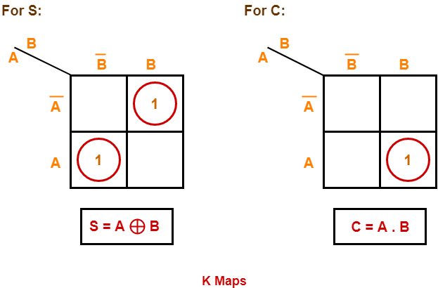
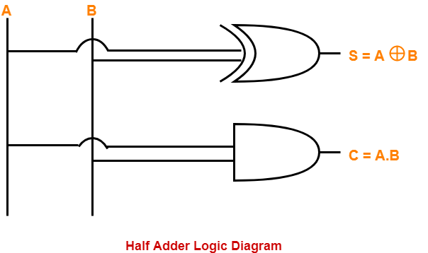
Half Adder-
Before you go through this article, make sure that you have gone through the previous article on Half Adder.
We have discussed-
- Half Adder is used for the purpose of adding two single bit numbers.
- Half adders have no scope of adding the carry bit resulting from the addition of previous bits.
- To overcome this drawback, full adder comes into play.

In this article, we will discuss about Full Adder.
Full Adder-
- Full Adder is a combinational logic circuit.
- It is used for the purpose of adding two single bit numbers with a carry.
- Thus, full adder has the ability to perform the addition of three bits.
- Full adder contains 3 inputs and 2 outputs (sum and carry) as shown-

Full Adder Designing-
Full adder is designed in the following steps-
Step-01:
Identify the input and output variables-
- Input variables = A, B, Cin (either 0 or 1)
- Output variables = S, Cout where S = Sum and Cout = Carry
Step-02:
Draw the truth table-
|
Inputs |
Outputs | |||
| A | B | Cin | Cout (Carry) | S (Sum) |
| 0 | 0 | 0 | 0 | 0 |
| 0 | 0 | 1 | 0 | 1 |
| 0 | 1 | 0 | 0 | 1 |
| 0 | 1 | 1 | 1 | 0 |
| 1 | 0 | 0 | 0 | 1 |
| 1 | 0 | 1 | 1 | 0 |
| 1 | 1 | 0 | 1 | 0 |
| 1 | 1 | 1 | 1 | 1 |
Truth Table
Step-03:
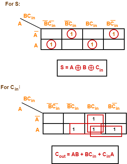
Draw K-maps using the above truth table and determine the simplified Boolean expressions-

Also Read- Full Subtractor
Step-04:
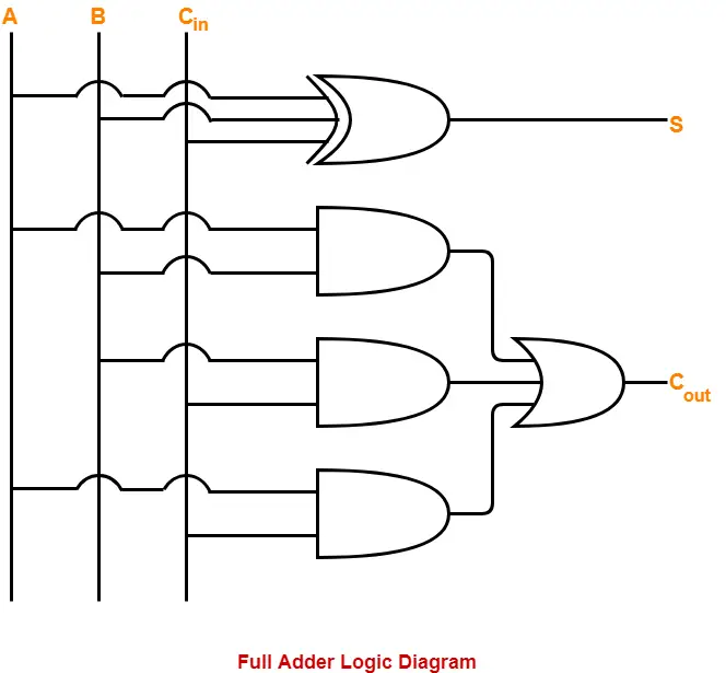
Draw the logic diagram.
The implementation of full adder using 1 XOR gate, 3 AND gates and 1 OR gate is as shown below-

To gain better understanding about Full Adder,
Next Article- Half Subtractor
Get more notes and other study material of Digital Design.
Watch video lectures by visiting our YouTube channel LearnVidFun.

