Latch-
A latch may be defined as-
| A latch is basically an unclocked flip flop.
OR
A latch is the basic building block using which clocked flip flops are constructed.
|
Latch Construction-
There are following two methods for constructing a latch-

- By using 2 NOR gates
- By using 2 NAND gates
1. Construction Of Latch By Using 2 NOR Gates-
Logic Circuit-
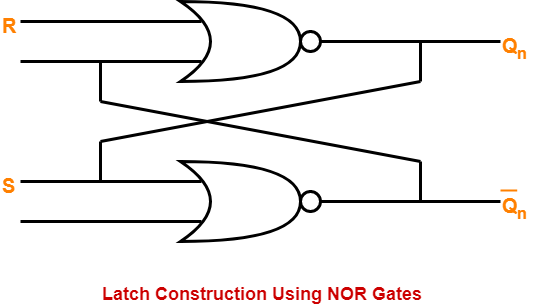
The logic circuit for a latch constructed using NOR gates is as shown below-

While constructing a latch using NOR gates, it is compulsory to consider-
- Reset input R in normal output Qn.
- Set input S in complemented output Q’n.
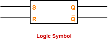
Logic Symbol-
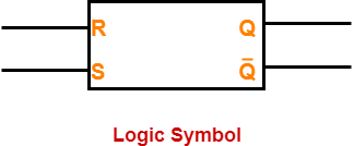
The logic symbol for a latch constructed using NOR gates is as shown below-

Truth Table-
The truth table for a latch constructed using NOR gates is as shown below-
| INPUTS |
OUTPUTS |
| R |
S |
Qn
(Present State)
|
Qn+1
(Next State)
|
| 0 |
0 |
0 |
0 |
| 0 |
0 |
1 |
1 |
| 0 |
1 |
0 |
1 |
| 0 |
1 |
1 |
1 |
| 1 |
0 |
0 |
0 |
| 1 |
0 |
1 |
0 |
| 1 |
1 |
0 |
Indeterminate |
| 1 |
1 |
1 |
Indeterminate |
Truth Table
The above truth table may be reduced as-
| INPUTS |
OUTPUTS |
REMARKS |
| R |
S |
Qn
(Present State)
|
Qn+1
(Next State)
|
States and Conditions |
| 0 |
0 |
X |
Qn
|
Hold state condition R = S = 0 |
| 0 |
1 |
X |
1 |
Set state condition R = 0 , S = 1 |
| 1 |
0 |
X |
0 |
Reset state condition R = 1 , S = 0 |
| 1 |
1 |
X |
Indeterminate |
Indeterminate state condition R = S = 1 |
Truth Table
2. Construction Of Latch By Using 2 NAND Gates-
Logic Circuit-
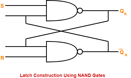
The logic circuit for a latch constructed using NAND gates is as shown below-

While constructing a latch using NAND gates, it is compulsory to consider-
- Set input S in normal output Qn.
- Reset input R in complemented output Q’n.
Logic Symbol-
The logic symbol for a latch constructed using NAND gates is as shown below-

Truth Table-
The truth table for a latch constructed using NAND gates is as shown below-
| INPUTS |
OUTPUTS |
| S |
R |
Qn
(Present State)
|
Qn+1
(Next State)
|
| 0 |
0 |
0 |
Indeterminate |
| 0 |
0 |
1 |
Indeterminate |
| 0 |
1 |
0 |
1 |
| 0 |
1 |
1 |
1 |
| 1 |
0 |
0 |
0 |
| 1 |
0 |
1 |
0 |
| 1 |
1 |
0 |
0 |
| 1 |
1 |
1 |
1 |
Truth Table
The above truth table may be reduced as-
| INPUTS |
OUTPUTS |
REMARKS |
| S |
R |
Qn
(Present State)
|
Qn+1
(Next State)
|
States and Conditions |
| 0 |
0 |
X |
Indeterminate |
Indeterminate state condition S = R = 0 |
| 0 |
1 |
X |
1 |
Set state condition S = 0 , R = 1 |
| 1 |
0 |
X |
0 |
Reset state condition S = 1 , R = 0 |
| 1 |
1 |
X |
Qn
|
Hold State condition S = R = 1 |
Truth Table
To gain better understanding about Latch in Digital Electronics,
Watch this Video Lecture
Next Article- Types of Flip-Flops
Get more notes and other study material of Digital Design.
Watch video lectures by visiting our YouTube channel LearnVidFun.

