Tag: Digital System Design Notes PDF

Half Subtractor | Definition | Circuit Diagram | Truth Table

Half Subtractor-


  • Half Subtractor is a combinational logic circuit.
  • It is used for the purpose of subtracting two single bit numbers.
  • It contains 2 inputs and 2 outputs (difference and borrow).


Half Subtractor Designing-


Half subtractor is designed in the following steps-


Step-01:


Identify the input and output variables-

  • Input variables = A, B (either 0 or 1)
  • Output variables = D, b where D = Difference and b = borrow


Step-02:


Draw the truth table-


Inputs Outputs
A B D (Difference) b (Borrow)
0 0 0 0
0 1 1 1
1 0 1 0
1 1 0 0

Truth Table


Step-03:


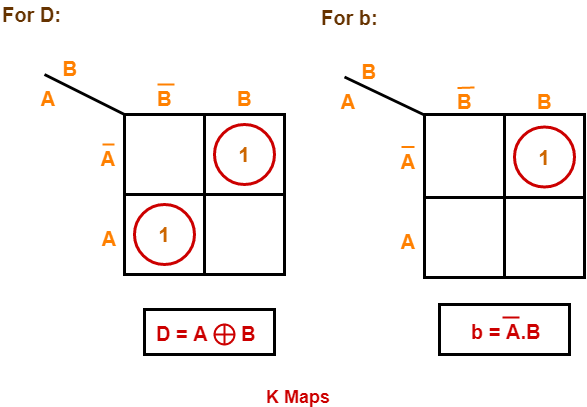
Draw K-maps using the above truth table and determine the simplified Boolean expressions-


Also Read- Half Adder


Step-04:


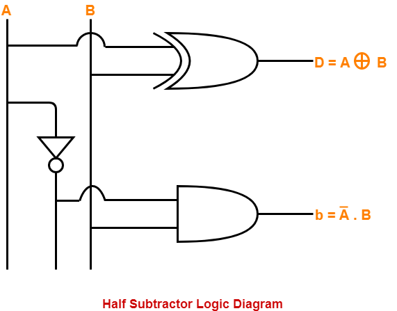
Draw the logic diagram.

The implementation of half subtractor using 1 XOR gate, 1 NOT gate and 1 AND gate is as shown below-


Limitation of Half Subtractor-


  • Half subtractors do not take into account “Borrow-in” from the previous circuit.
  • This is a major drawback of half subtractors.
  • This is because real time scenarios involve subtracting the multiple number of bits which can not be accomplished using half subtractors.


To overcome this drawback, Full Subtractor comes into play.


To gain better understanding about Half Subtractor,

Watch this Video Lecture


Next Article- Full Subtractor


Get more notes and other study material of Digital Design.

Watch video lectures by visiting our YouTube channel LearnVidFun.

Full Adder | Definition | Circuit Diagram | Truth Table

Half Adder-


Before you go through this article, make sure that you have gone through the previous article on Half Adder.


We have discussed-

  • Half Adder is used for the purpose of adding two single bit numbers.
  • Half adders have no scope of adding the carry bit resulting from the addition of previous bits.
  • To overcome this drawback, full adder comes into play.


In this article, we will discuss about Full Adder.


Full Adder-


  • Full Adder is a combinational logic circuit.
  • It is used for the purpose of adding two single bit numbers with a carry.
  • Thus, full adder has the ability to perform the addition of three bits.
  • Full adder contains 3 inputs and 2 outputs (sum and carry) as shown-


Full Adder Designing-


Full adder is designed in the following steps-


Step-01:


Identify the input and output variables-

  • Input variables = A, B, Cin (either 0 or 1)
  • Output variables = S, Cout where S = Sum and Cout = Carry


Step-02:


Draw the truth table-


Inputs
Outputs
A B Cin Cout (Carry) S (Sum)
0 0 0 0 0
0 0 1 0 1
0 1 0 0 1
0 1 1 1 0
1 0 0 0 1
1 0 1 1 0
1 1 0 1 0
1 1 1 1 1

Truth Table


Step-03:


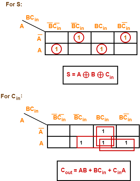
Draw K-maps using the above truth table and determine the simplified Boolean expressions-


Also Read- Full Subtractor


Step-04:


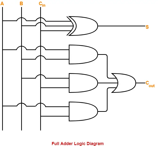
Draw the logic diagram.

The implementation of full adder using 1 XOR gate, 3 AND gates and 1 OR gate is as shown below-


To gain better understanding about Full Adder,

Watch this Video Lecture


Next Article- Half Subtractor


Get more notes and other study material of Digital Design.

Watch video lectures by visiting our YouTube channel LearnVidFun.

Half Adder | Definition | Circuit Diagram | Truth Table

Half Adder-


  • Half Adder is a combinational logic circuit.
  • It is used for the purpose of adding two single bit numbers.
  • It contains 2 inputs and 2 outputs (sum and carry).


Half Adder Designing-


Half adder is designed in the following steps-


Step-01:


Identify the input and output variables-

  • Input variables = A, B (either 0 or 1)
  • Output variables = S, C where S = Sum and C = Carry


Step-02:


Draw the truth table-


Inputs Outputs
A B C (Carry) S (Sum)
0 0 0 0
0 1 0 1
1 0 0 1
1 1 1 0

Truth Table


Step-03:


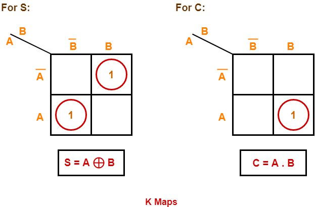
Draw K-maps using the above truth table and determine the simplified Boolean expressions-


Also Read- Half Subtractor


Step-04:


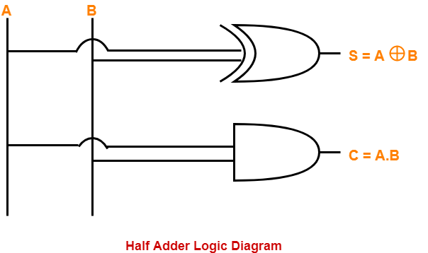
Draw the logic diagram.

The implementation of half adder using 1 XOR gate and 1 AND gate is as shown below-


Limitation of Half Adder-


  • Half adders have no scope of adding the carry bit resulting from the addition of previous bits.
  • This is a major drawback of half adders.
  • This is because real time scenarios involve adding the multiple number of bits which can not be accomplished using half adders.


To overcome this drawback, Full Adder comes into play.


To gain better understanding about Half Adder,

Watch this Video Lecture


Next Article- Full Adder


Get more notes and other study material of Digital Design.

Watch video lectures by visiting our YouTube channel LearnVidFun.

JK Flip Flop | Diagram | Truth Table | Excitation Table

Flip Flops-


Before you go through this article, make sure that you have gone through the previous article on Flip Flops.


We have discussed-

  • A Flip Flop is a memory element that is capable of storing one bit of information.
  • It is also called as Bistable Multivibrator since it has two stable states either 0 or 1.


There are following 4 basic types of flip flops-
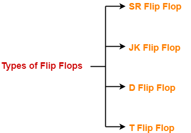


  1. SR Flip Flop
  2. JK Flip Flop
  3. D Flip Flop
  4. T Flip Flop


In this article, we will discuss about JK Flip Flop.


JK Flip Flop-


JK flip flop is a refined & improved version of SR Flip Flop

that has been introduced to solve the problem of indeterminate state

that occurs in SR flip flop when both the inputs are 1.


In JK flip flop,

  • Input J behaves like input S of SR flip flop which was meant to set the flip flop.
  • Input K behaves like input R of SR flip flop which was meant to reset the flip flop.


Construction of JK Flip Flop-


There are following two methods for constructing a JK flip flop-


  1. By using SR flip flop constructed from NOR latch
  2. By using SR flip flop constructed from NAND latch


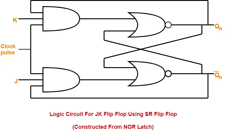
1. Construction of JK Flip Flop By Using SR Flip Flop Constructed From NOR Latch-


This method of constructing JK Flip Flop uses-

  • SR Flip Flop constructed from NOR latch
  • Two other connections


Logic Circuit-


The logic circuit for JK Flip Flop constructed using SR Flip Flop constructed from NOR latch is as shown below-


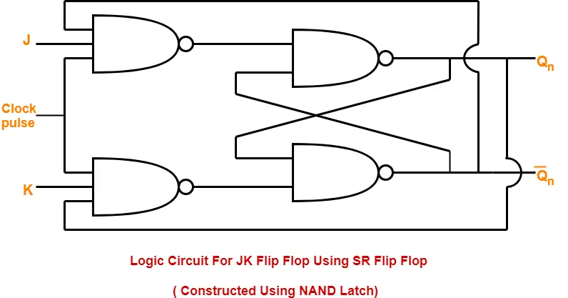
2. Construction of JK Flip Flop By Using SR Flip Flop Constructed From NAND Latch-


This method of constructing JK Flip Flop uses-

  • SR Flip Flop constructed from NAND latch
  • Two other connections


Logic Circuit-


The logic circuit for JK Flip Flop constructed using SR Flip Flop constructed from NAND latch is as shown below-


Logic Symbol-


The logic symbol for JK Flip Flop is as shown below-


Truth Table-


The truth table for JK Flip Flop is as shown below-


INPUTS OUTPUTS
J K Qn

(Present State)

Qn+1

(Next State)

0 0 0 0
0 0 1 1
0 1 0 0
0 1 1 0
1 0 0 1
1 0 1 1
1 1 0 1
1 1 1 0

Truth Table


The above truth table may be reduced as-


INPUTS OUTPUTS REMARKS
J K Qn

(Present State)

Qn+1

(Next State)

States and Conditions
0 0 X Qn Hold State condition J = K = 0
0 1 X 0 Reset state condition J = 0 , K = 1
1 0 X 1 Set state condition J = 1 , K = 0
1 1 X Q’n Toggle state condition J = K = 1

Truth Table


Characteristic Equation-


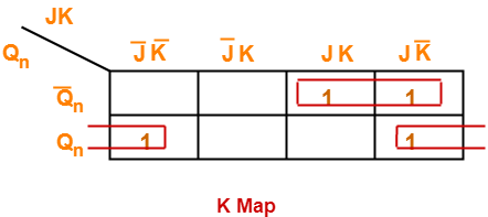
Draw a k map using the above truth table-


From here-

Qn+1 = Q’n (JK + JK’) + Qn (J’K’ + JK’)


Qn+1 = Q’nJ + QnK’


Excitation Table-


The excitation table of any flip flop is drawn using its truth table.


What is excitation table?

For a given combination of present state Qn and next state Qn+1, excitation table tell the inputs required.


Qn Qn+1 S R
0 0 0 X
0 1 1 X
1 0 X 1
1 1 X 0

Excitation Table


SR Flip Flop Vs JK Flip Flop-


Both JK flip flop and SR flip flop are functionally same.

The only difference between them is-

  • In JK flip flop, indeterminate state does not occur.
  • In JK flip flop, instead of indeterminate state, the present state toggles.
  • In other words, the present state gets inverted when both the inputs are 1.


To gain better understanding about JK Flip Flop,

Watch this Video Lecture


Next Article- Half Adder


Get more notes and other study material of Digital Design.

Watch video lectures by visiting our YouTube channel LearnVidFun.

SR Flip Flop | Diagram | Truth Table | Excitation Table

Flip Flops-


Before you go through this article, make sure that you have gone through the previous article on Flip Flops.


We have discussed-

  • A Flip Flop is a memory element that is capable of storing one bit of information.
  • It is also called as Bistable Multivibrator since it has two stable states either 0 or 1.


There are following 4 basic types of flip flops-


  1. SR Flip Flop
  2. JK Flip Flop
  3. D Flip Flop
  4. T Flip Flop


In this article, we will discuss about SR Flip Flop.


SR Flip Flop-


  • SR flip flop is the simplest type of flip flops.
  • It stands for Set Reset flip flop.
  • It is a clocked flip flop.


Construction of SR Flip Flop-


There are following two methods for constructing a SR flip flop-


  1. By using NOR latch
  2. By using NAND latch


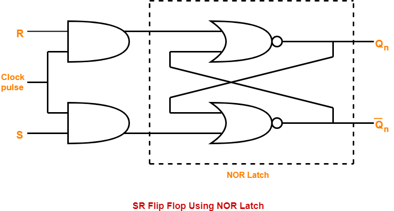
1. Construction of SR Flip Flop By Using NOR Latch-


This method of constructing SR Flip Flop uses-

  • NOR latch
  • Two AND gates


Logic Circuit-


The logic circuit for SR Flip Flop constructed using NOR latch is as shown below-


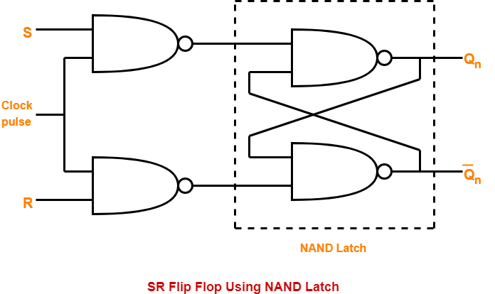
2. Construction of SR Flip Flop By Using NAND Latch-


This method of constructing SR Flip Flop uses-

  • NAND latch
  • Two NAND gates


Logic Circuit-


The logic circuit for SR Flip Flop constructed using NAND latch is as shown below-


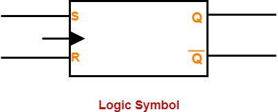
Logic Symbol-


The logic symbol for SR Flip Flop is as shown below-


Truth Table-


The truth table for SR Flip Flop is as shown below-


INPUTS OUTPUTS
S R Qn

(Present State)

Qn+1

(Next State)

0 0 0 0
0 0 1 1
0 1 0 0
0 1 1 0
1 0 0 1
1 0 1 1
1 1 0 Indeterminate
1 1 1 Indeterminate

Truth Table


The above truth table may be reduced as-


INPUTS OUTPUTS REMARKS
S R Qn

(Present State)

Qn+1

(Next State)

States and Conditions
0 0 X Qn Hold State condition S = R = 0
0 1 X 0 Reset state condition S = 0 , R = 1
1 0 X 1 Set state condition S = 1 , R = 0
1 1 X Indeterminate Indeterminate state condition S = R = 1

Truth Table


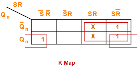
Characteristic Equation-


Draw a k map using the above truth table-


From here-

Qn+1 = ( SR + SR’ ) ( Qn +  Q’n ) + Qn ( S’R’ + SR’ )


Qn+1 = S + QnR’


Excitation Table-


The excitation table of any flip flop is drawn using its truth table.


What is excitation table?

For a given combination of present state Qn and next state Qn+1, excitation table tell the inputs required.


Qn Qn+1 S R
0 0 0 X
0 1 1 0
1 0 0 1
1 1 X 0

Excitation Table


To gain better understanding about SR Flip Flop,

Watch this Video Lecture


Next Article- JK Flip Flop


Get more notes and other study material of Digital Design.

Watch video lectures by visiting our YouTube channel LearnVidFun.