Logic Gates-
Logic Gates may be defined as-
| Logic gates are the digital circuits capable of performing a particular logic function
by operating on a number of binary inputs. OR Logic gates are the basic building blocks of any digital circuit. |
Types Of Logic Gates-
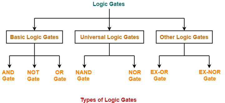
Logic gates can be broadly classified as-

In this article, we will discuss about Basic Logic Gates.
Basic Logic Gates-
Basic Logic Gates are the fundamental logic gates using which universal logic gates and other logic gates are constructed.
They have the following properties-
- Basic logic gates are associative in nature.
- Basic logic gates are commutative in nature.
There are following three basic logic gates-
- AND Gate
- OR Gate
- NOT Gate
1. AND Gate-
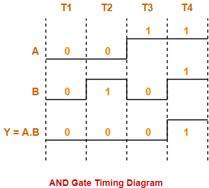
- The output of AND gate is high (‘1’) if all of its inputs are high (‘1’).
- The output of AND gate is low (‘0’) if any one of its inputs is low (‘0’).
Logic Symbol-
The logic symbol for AND Gate is as shown below-

Truth Table-
The truth table for AND Gate is as shown below-
| A | B | Y = A.B |
| 0 | 0 | 0 |
| 0 | 1 | 0 |
| 1 | 0 | 0 |
| 1 | 1 | 1 |
Truth Table
Timing Diagram-
The timing diagram for AND Gate is as shown below-
2. OR Gate-
- The output of OR gate is high (‘1’) if any one of its inputs is high (‘1’).
- The output of OR gate is low (‘0’) if all of its inputs are low (‘0’).
Logic Symbol-
The logic symbol for OR Gate is as shown below-

Truth Table-
The truth table for OR Gate is as shown below-
| A | B | Y = A + B |
| 0 | 0 | 0 |
| 0 | 1 | 1 |
| 1 | 0 | 1 |
| 1 | 1 | 1 |
Truth Table
Timing Diagram-
The timing diagram for OR Gate is as shown below-

Also Read- Alternative Logic Gates
3. NOT Gate-
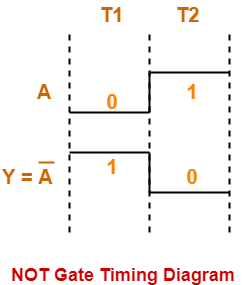
- The output of NOT gate is high (‘1’) if its input is low (‘0’).
- The output of NOT gate is low (‘0’) if its input is high (‘1’).
From here-
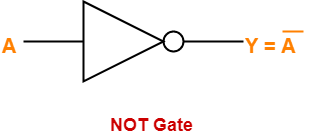
- It is clear that NOT gate simply inverts the given input.
- Since NOT gate simply inverts the given input, therefore it is also known as Inverter Gate.
Logic Symbol-
The logic symbol for NOT Gate is as shown below-
Truth Table-
The truth table for NOT Gate is as shown below-
| A | Y = A’ |
| 0 | 1 |
| 1 | 0 |
Truth Table
Timing Diagram-
The timing diagram for NOT Gate is as shown below-
To gain better understanding about Logic Gates,
Next Article- Universal Logic Gates
Get more notes and other study material of Digital Design.
Watch video lectures by visiting our YouTube channel LearnVidFun.
