Category: Computer Organization and Architecture

Direct Mapping | Cache | Practice Problems

Direct Mapping-


Before you go through this article, make sure that you have gone through the previous article on Direct Mapping.


In direct mapping,

  • A particular block of main memory can be mapped to one particular cache line only.
  • Block ‘j’ of main memory will map to line number (j mod number of cache lines) of the cache.
  • There is no need of any replacement algorithm.


In this article, we will discuss practice problems based on direct mapping.


Also Read- Cache Mapping Techniques


PRACTICE PROBLEMS BASED ON DIRECT MAPPING-


Problem-01:


Consider a direct mapped cache of size 16 KB with block size 256 bytes. The size of main memory is 128 KB. Find-

  1. Number of bits in tag
  2. Tag directory size


Solution-


Given-

  • Cache memory size = 16 KB
  • Block size = Frame size = Line size = 256 bytes
  • Main memory size = 128 KB


We consider that the memory is byte addressable.


Number of Bits in Physical Address-


We have,

Size of main memory

= 128 KB

= 217 bytes

Thus, Number of bits in physical address = 17 bits


Number of Bits in Block Offset-


We have,

Block size

= 256 bytes

= 28 bytes

Thus, Number of bits in block offset = 8 bits


Number of Bits in Line Number-


Total number of lines in cache

= Cache size / Line size

= 16 KB / 256 bytes

= 214 bytes / 28 bytes

= 26 lines

Thus, Number of bits in line number = 6 bits


Number of Bits in Tag-


Number of bits in tag

= Number of bits in physical address – (Number of bits in line number + Number of bits in block offset)

= 17 bits – (6 bits + 8 bits)

= 17 bits – 14 bits

= 3 bits

Thus, Number of bits in tag = 3 bits


Tag Directory Size-


Tag directory size

= Number of tags x Tag size

= Number of lines in cache x Number of bits in tag

= 26 x 3 bits

= 192 bits

= 24 bytes

Thus, size of tag directory = 24 bytes


Problem-02:


Consider a direct mapped cache of size 512 KB with block size 1 KB. There are 7 bits in the tag. Find-

  1. Size of main memory
  2. Tag directory size


Solution-


Given-

  • Cache memory size = 512 KB
  • Block size = Frame size = Line size = 1 KB
  • Number of bits in tag = 7 bits


We consider that the memory is byte addressable.


Number of Bits in Block Offset-


We have,

Block size

= 1 KB

= 210 bytes

Thus, Number of bits in block offset = 10 bits


Number of Bits in Line Number-


Total number of lines in cache

= Cache size / Line size

= 512 KB / 1 KB

= 29 lines

Thus, Number of bits in line number = 9 bits


Number of Bits in Physical Address-


Number of bits in physical address

= Number of bits in tag + Number of bits in line number + Number of bits in block offset

= 7 bits + 9 bits + 10 bits

= 26 bits

Thus, Number of bits in physical address = 26 bits


Size of Main Memory-


We have,

Number of bits in physical address = 26 bits

Thus, Size of main memory

= 226 bytes

= 64 MB


Tag Directory Size-


Tag directory size

= Number of tags x Tag size

= Number of lines in cache x Number of bits in tag

= 29 x 7 bits

= 3584 bits

= 448 bytes

Thus, size of tag directory = 448 bytes


Problem-03:


Consider a direct mapped cache with block size 4 KB. The size of main memory is 16 GB and there are 10 bits in the tag. Find-

  1. Size of cache memory
  2. Tag directory size


Solution-


Given-

  • Block size = Frame size = Line size = 4 KB
  • Size of main memory = 16 GB
  • Number of bits in tag = 10 bits


We consider that the memory is byte addressable.


Number of Bits in Physical Address-


We have,

Size of main memory

= 16 GB

= 234 bytes

Thus, Number of bits in physical address = 34 bits


Number of Bits in Block Offset-


We have,

Block size

= 4 KB

= 212 bytes

Thus, Number of bits in block offset = 12 bits


Number of Bits in Line Number-


Number of bits in line number

= Number of bits in physical address – (Number of bits in tag + Number of bits in block offset)

= 34 bits – (10 bits + 12 bits)

= 34 bits – 22 bits

= 12 bits

Thus, Number of bits in line number = 12 bits


Number of Lines in Cache-


We have-

Number of bits in line number = 12 bits

Thus, Total number of lines in cache = 212 lines


Size of Cache Memory-


Size of cache memory

= Total number of lines in cache x Line size

= 212 x 4 KB

= 214 KB

= 16 MB

Thus, Size of cache memory = 16 MB


Tag Directory Size-


Tag directory size

= Number of tags x Tag size

= Number of lines in cache x Number of bits in tag

= 212 x 10 bits

= 40960 bits

= 5120 bytes

Thus, size of tag directory = 5120 bytes


Also Read- Practice Problems On Set Associative Mapping


Problem-04:


Consider a direct mapped cache of size 32 KB with block size 32 bytes. The CPU generates 32 bit addresses. The number of bits needed for cache indexing and the number of tag bits are respectively-

  1. 10, 17
  2. 10, 22
  3. 15, 17
  4. 5, 17


Solution-


Given-

  • Cache memory size = 32 KB
  • Block size = Frame size = Line size = 32 bytes
  • Number of bits in physical address = 32 bits


Number of Bits in Block Offset-


We have,

Block size

= 32 bytes

= 25 bytes

Thus, Number of bits in block offset = 5 bits


Number of Bits in Line Number-


Total number of lines in cache

= Cache size / Line size

= 32 KB / 32 bytes

= 210 lines

Thus, Number of bits in line number = 10 bits


Number of Bits Required For Cache Indexing-


Number of bits required for cache indexing

= Number of bits in line number

= 10 bits


Number Of Bits in Tag-


Number of bits in tag

= Number of bits in physical address – (Number of bits in line number + Number of bits in block offset)

= 32 bits – (10 bits + 5 bits)

= 32 bits – 15 bits

= 17 bits

Thus, Number of bits in tag = 17 bits


Thus, Option (A) is correct.


Problem-05:


Consider a machine with a byte addressable main memory of 232 bytes divided into blocks of size 32 bytes. Assume that a direct mapped cache having 512 cache lines is used with this machine. The size of the tag field in bits is ______.


Solution-


Given-

  • Main memory size = 232 bytes
  • Block size = Frame size = Line size = 32 bytes
  • Number of lines in cache = 512 lines


Number of Bits in Physical Address-


We have,

Size of main memory

= 232 bytes

Thus, Number of bits in physical address = 32 bits


Number of Bits in Block Offset-


We have,

Block size

= 32 bytes

= 25 bytes

Thus, Number of bits in block offset = 5 bits


Number of Bits in Line Number-


Total number of lines in cache

= 512 lines

= 29 lines

Thus, Number of bits in line number = 9 bits


Number Of Bits in Tag-


Number of bits in tag

= Number of bits in physical address – (Number of bits in line number + Number of bits in block offset)

= 32 bits – (9 bits + 5 bits)

= 32 bits – 14 bits

= 18 bits

Thus, Number of bits in tag = 18 bits


Problem-06:


An 8 KB direct-mapped write back cache is organized as multiple blocks, each of size 32 bytes. The processor generates 32 bit addresses. The cache controller maintains the tag information for each cache block comprising of the following-

  • 1 valid bit
  • 1 modified bit
  • As many bits as the minimum needed to identify the memory block mapped in the cache

What is the total size of memory needed at the cache controller to store meta data (tags) for the cache?

  1. 4864 bits
  2. 6144 bits
  3. 6656 bits
  4. 5376 bits


Solution-


Given-

  • Cache memory size = 8 KB
  • Block size = Frame size = Line size = 32 bytes
  • Number of bits in physical address = 32 bits


Number of Bits in Block Offset-


We have,

Block size

= 32 bytes

= 25 bytes

Thus, Number of bits in block offset = 5 bits


Number of Bits in Line Number-


Total number of lines in cache

= Cache memory size / Line size

= 8 KB / 32 bytes

= 213 bytes / 25 bytes

= 28 lines

Thus, Number of bits in line number = 8 bits


Number Of Bits in Tag-


Number of bits in tag

= Number of bits in physical address – (Number of bits in line number + Number of bits in block offset)

= 32 bits – (8 bits + 5 bits)

= 32 bits – 13 bits

= 19 bits

Thus, Number of bits in tag = 19 bits


Memory Size Needed At Cache Controller-


Size of memory needed at cache controller

= Number of lines in cache x (1 valid bit + 1 modified bit + 19 bits to identify block)

= 28 x 21 bits

= 5376 bits


To watch video solutions and practice more problems,

Watch this Video Lecture


Next Article- Practice Problems On Fully Associative Mapping


Get more notes and other study material of Computer Organization and Architecture.

Watch video lectures by visiting our YouTube channel LearnVidFun.

Direct Mapping | Direct Mapped Cache

Cache Mapping-


Before you go through this article, make sure that you have gone through the previous article on Cache Mapping.


Cache mapping is a technique by which the contents of main memory are brought into the cache memory.


Different cache mapping techniques are-


  1. Direct Mapping
  2. Fully Associative Mapping
  3. K-way Set Associative Mapping


In this article, we will discuss about direct mapping in detail.


Direct Mapping-


In direct mapping,

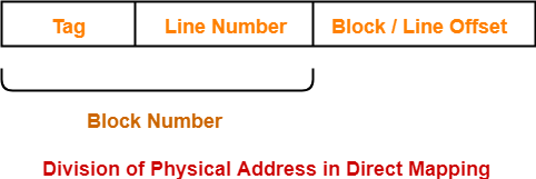
  • A particular block of main memory can map to only one particular line of the cache.
  • The line number of cache to which a particular block can map is given by-


Cache line number

= ( Main Memory Block Address ) Modulo (Number of lines in Cache)


Division of Physical Address-


In direct mapping, the physical address is divided as-


Direct Mapped Cache-


Direct mapped cache employs direct cache mapping technique.


The following steps explain the working of direct mapped cache-


After CPU generates a memory request,

  • The line number field of the address is used to access the particular line of the cache.
  • The tag field of the CPU address is then compared with the tag of the line.
  • If the two tags match, a cache hit occurs and the desired word is found in the cache.
  • If the two tags do not match, a cache miss occurs.
  • In case of a cache miss, the required word has to be brought from the main memory.
  • It is then stored in the cache together with the new tag replacing the previous one.


Implementation-


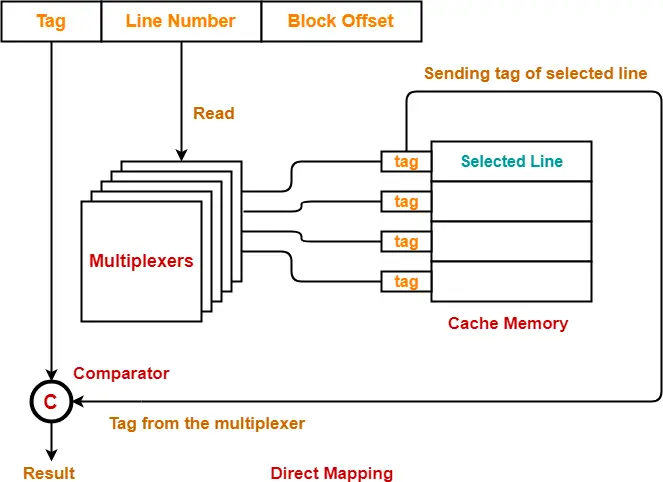
The following diagram shows the implementation of direct mapped cache-


(For simplicity, this diagram shows does not show all the lines of multiplexers)


The steps involved are as follows-


Step-01:


  • Each multiplexer reads the line number from the generated physical address using its select lines in parallel.
  • To read the line number of L bits, number of select lines each multiplexer must have = L.


Step-02:


  • After reading the line number, each multiplexer goes to the corresponding line in the cache memory using its input lines in parallel.
  • Number of input lines each multiplexer must have = Number of lines in the cache memory


Step-03:


  • Each multiplexer outputs the tag bit it has selected from that line to the comparator using its output line.
  • Number of output line in each multiplexer = 1.


UNDERSTAND


It is important to understand-

  • A multiplexer can output only a single bit on output line.
  • So, to output the complete tag to the comparator,

Number of multiplexers required = Number of bits in the tag

  • Each multiplexer is configured to read the tag bit at specific location.


Example-


  • 1st multiplexer is configured to output the first bit of the tag.
  • 2nd multiplexer is configured to output the second bit of the tag.
  • 3rd multiplexer is configured to output the third bit of the tag and so on.

So,

  • Each multiplexer selects the tag bit of the selected line for which it has been configured and outputs on the output line.
  • The complete tag as a whole is sent to the comparator for comparison in parallel.


Step-04:


  • Comparator compares the tag coming from the multiplexers with the tag of the generated address.
  • Only one comparator is required for the comparison where-

Size of comparator = Number of bits in the tag

  • If the two tags match, a cache hit occurs otherwise a cache miss occurs.


Hit latency-


The time taken to find out whether the required word is present in the Cache Memory or not is called as hit latency.


For direct mapped cache,

Hit latency = Multiplexer latency + Comparator latency


Also Read- Set Associative Cache | Implementation & Formulas


Important Results-


Following are the few important results for direct mapped cache-

  • Block j of main memory can map to line number (j mod number of lines in cache) only of the cache.
  • Number of multiplexers required = Number of bits in the tag
  • Size of each multiplexer = Number of lines in cache x 1
  • Number of comparators required = 1
  • Size of comparator = Number of bits in the tag
  • Hit latency = Multiplexer latency + Comparator latency


To gain better understanding about direct mapping,

Watch this Video Lecture


Next Article- Practice Problems On Direct Mapping


Get more notes and other study material of Computer Organization and Architecture.

Watch video lectures by visiting our YouTube channel LearnVidFun.
Cache Mapping | Cache Mapping Techniques

Cache Memory-


Before you go through this article, make sure that you have gone through the previous article on Cache Memory.


We have discussed-


Cache memory bridges the speed mismatch between the processor and the main memory.


When cache hit occurs,

  • The required word is present in the cache memory.
  • The required word is delivered to the CPU from the cache memory.


When cache miss occurs,

  • The required word is not present in the cache memory.
  • The page containing the required word has to be mapped from the main memory.
  • This mapping is performed using cache mapping techniques.


In this article, we will discuss different cache mapping techniques.


Cache Mapping-


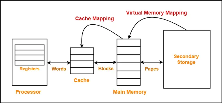
  • Cache mapping defines how a block from the main memory is mapped to the cache memory in case of a cache miss.

OR

  • Cache mapping is a technique by which the contents of main memory are brought into the cache memory.


The following diagram illustrates the mapping process-


Now, before proceeding further, it is important to note the following points-


NOTES


  • Main memory is divided into equal size partitions called as blocks or frames.
  • Cache memory is divided into partitions having same size as that of blocks called as lines.
  • During cache mapping, block of main memory is simply copied to the cache and the block is not actually brought from the main memory.


Cache Mapping Techniques-


Cache mapping is performed using following three different techniques-


  1. Direct Mapping
  2. Fully Associative Mapping
  3. K-way Set Associative Mapping


1. Direct Mapping-


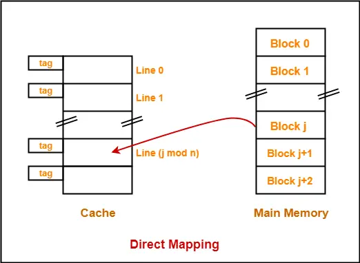
In direct mapping,

  • A particular block of main memory can map only to a particular line of the cache.
  • The line number of cache to which a particular block can map is given by-


Cache line number

= ( Main Memory Block Address ) Modulo (Number of lines in Cache)


Example-


  • Consider cache memory is divided into ‘n’ number of lines.
  • Then, block ‘j’ of main memory can map to line number (j mod n) only of the cache.


Need of Replacement Algorithm-


In direct mapping,

  • There is no need of any replacement algorithm.
  • This is because a main memory block can map only to a particular line of the cache.
  • Thus, the new incoming block will always replace the existing block (if any) in that particular line.


Division of Physical Address-


In direct mapping, the physical address is divided as-


2. Fully Associative Mapping-


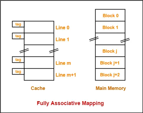
In fully associative mapping,

  • A block of main memory can map to any line of the cache that is freely available at that moment.
  • This makes fully associative mapping more flexible than direct mapping.


Example-


Consider the following scenario-


Here,

  • All the lines of cache are freely available.
  • Thus, any block of main memory can map to any line of the cache.
  • Had all the cache lines been occupied, then one of the existing blocks will have to be replaced.


Need of Replacement Algorithm-


In fully associative mapping,

  • A replacement algorithm is required.
  • Replacement algorithm suggests the block to be replaced if all the cache lines are occupied.
  • Thus, replacement algorithm like FCFS Algorithm, LRU Algorithm etc is employed.


Division of Physical Address-


In fully associative mapping, the physical address is divided as-


3. K-way Set Associative Mapping-


In k-way set associative mapping,

  • Cache lines are grouped into sets where each set contains k number of lines.
  • A particular block of main memory can map to only one particular set of the cache.
  • However, within that set, the memory block can map any cache line that is freely available.
  • The set of the cache to which a particular block of the main memory can map is given by-


Cache set number

= ( Main Memory Block Address ) Modulo (Number of sets in Cache)


Also Read- Set Associative Mapping | Implementation and Formulas


Example-


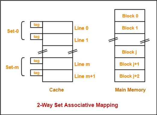
Consider the following example of 2-way set associative mapping-


Here,

  • k = 2 suggests that each set contains two cache lines.
  • Since cache contains 6 lines, so number of sets in the cache = 6 / 2 = 3 sets.
  • Block ‘j’ of main memory can map to set number (j mod 3) only of the cache.
  • Within that set, block ‘j’ can map to any cache line that is freely available at that moment.
  • If all the cache lines are occupied, then one of the existing blocks will have to be replaced.


Need of Replacement Algorithm-


  • Set associative mapping is a combination of direct mapping and fully associative mapping.
  • It uses fully associative mapping within each set.
  • Thus, set associative mapping requires a replacement algorithm.


Division of Physical Address-


In set associative mapping, the physical address is divided as-


Special Cases-


  • If k = 1, then k-way set associative mapping becomes direct mapping i.e.


1-way Set Associative Mapping ≡ Direct Mapping


  • If k = Total number of lines in the cache, then k-way set associative mapping becomes fully associative mapping.


Next Article- Direct Mapping | Implementation & Formulas


Get more notes and other study material of Computer Organization and Architecture.

Watch video lectures by visiting our YouTube channel LearnVidFun.
Addressing Modes | Types of Addressing Modes

Addressing Modes-


The different ways of specifying the location of an operand in an instruction are called as addressing modes.


Types of Addressing Modes-


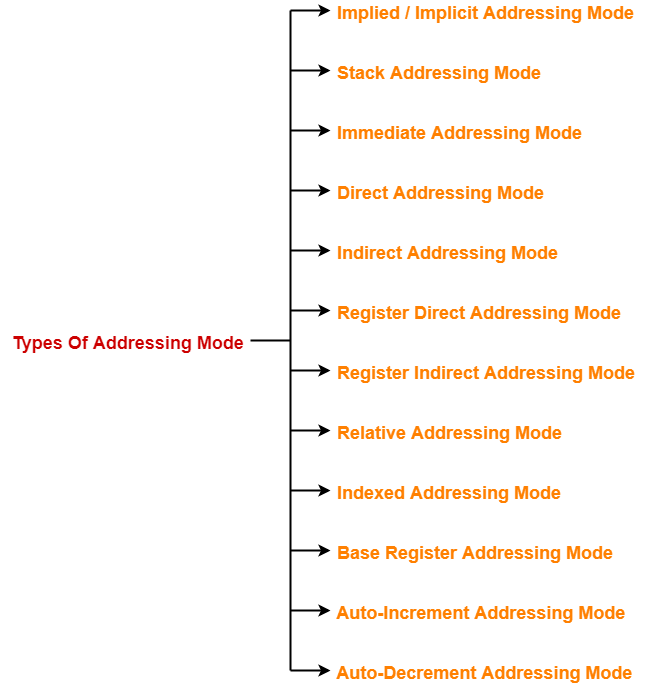
In computer architecture, there are following types of addressing modes-


  1. Implied / Implicit Addressing Mode
  2. Stack Addressing Mode
  3. Immediate Addressing Mode
  4. Direct Addressing Mode
  5. Indirect Addressing Mode
  6. Register Direct Addressing Mode
  7. Register Indirect Addressing Mode
  8. Relative Addressing Mode
  9. Indexed Addressing Mode
  10. Base Register Addressing Mode
  11. Auto-Increment Addressing Mode
  12. Auto-Decrement Addressing Mode


In this article, we will discuss about these addressing modes in detail.


1. Implied Addressing Mode-


In this addressing mode,

  • The definition of the instruction itself specify the operands implicitly.
  • It is also called as implicit addressing mode.


Examples-


  • The instruction “Complement Accumulator” is an implied mode instruction.
  • In a stack organized computer, Zero Address Instructions are implied mode instructions.

(since operands are always implied to be present on the top of the stack)


2. Stack Addressing Mode-


In this addressing mode,

  • The operand is contained at the top of the stack.


Example-


ADD

  • This instruction simply pops out two symbols contained at the top of the stack.
  • The addition of those two operands is performed.
  • The result so obtained after addition is pushed again at the top of the stack.


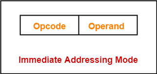
3. Immediate Addressing Mode-


In this addressing mode,

  • The operand is specified in the instruction explicitly.
  • Instead of address field, an operand field is present that contains the operand.


Examples-


  • ADD 10 will increment the value stored in the accumulator by 10.
  • MOV R #20 initializes register R to a constant value 20.


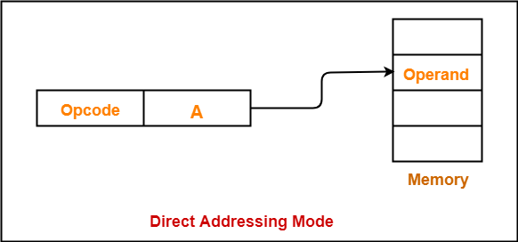
4. Direct Addressing Mode-


In this addressing mode,

  • The address field of the instruction contains the effective address of the operand.
  • Only one reference to memory is required to fetch the operand.
  • It is also called as absolute addressing mode.


Example-


  • ADD X will increment the value stored in the accumulator by the value stored at memory location X.

AC ← AC + [X]


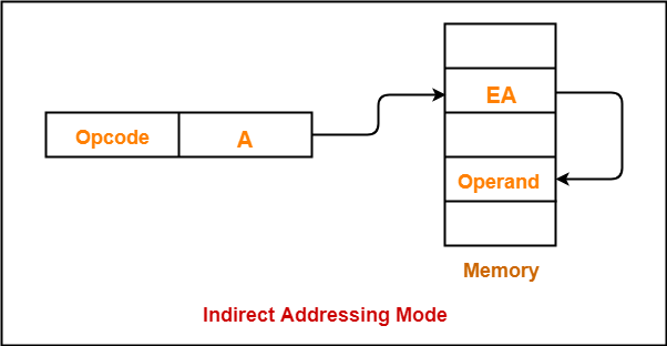
5. Indirect Addressing Mode-


In this addressing mode,

  • The address field of the instruction specifies the address of memory location that contains the effective address of the operand.
  • Two references to memory are required to fetch the operand.


Example-


  • ADD X will increment the value stored in the accumulator by the value stored at memory location specified by X.

AC ← AC + [[X]]


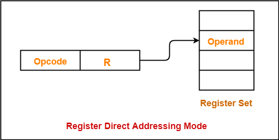
6. Register Direct Addressing Mode-


In this addressing mode,

  • The operand is contained in a register set.
  • The address field of the instruction refers to a CPU register that contains the operand.
  • No reference to memory is required to fetch the operand.


Example-


  • ADD R will increment the value stored in the accumulator by the content of register R.

AC ← AC + [R]


NOTE-


It is interesting to note-

  • This addressing mode is similar to direct addressing mode.
  • The only difference is address field of the instruction refers to a CPU register instead of main memory.


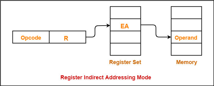
7. Register Indirect Addressing Mode-


In this addressing mode,

  • The address field of the instruction refers to a CPU register that contains the effective address of the operand.
  • Only one reference to memory is required to fetch the operand.


Example-


  • ADD R will increment the value stored in the accumulator by the content of memory location specified in register R.

AC ← AC + [[R]]


NOTE-


It is interesting to note-

  • This addressing mode is similar to indirect addressing mode.
  • The only difference is address field of the instruction refers to a CPU register.


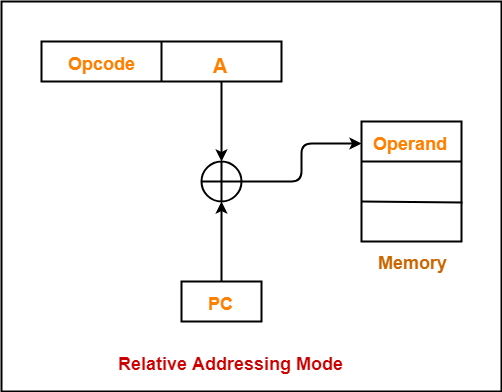
8. Relative Addressing Mode-


In this addressing mode,

  • Effective address of the operand is obtained by adding the content of program counter with the address part of the instruction.


Effective Address

= Content of Program Counter + Address part of the instruction


NOTE-


  • Program counter (PC) always contains the address of the next instruction to be executed.
  • After fetching the address of the instruction, the value of program counter immediately increases.
  • The value increases irrespective of whether the fetched instruction has completely executed or not.


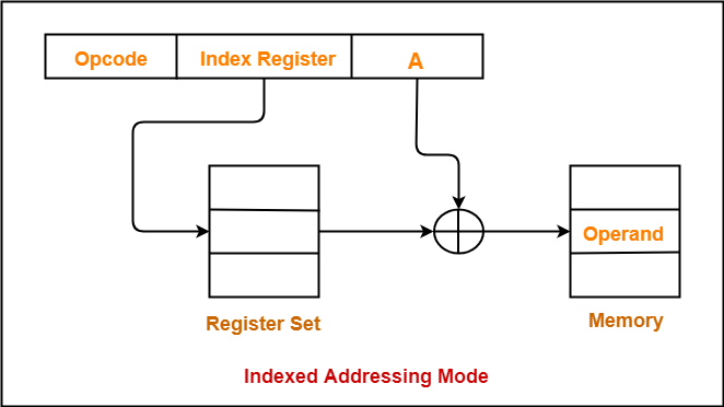
9. Indexed Addressing Mode-


In this addressing mode,

  • Effective address of the operand is obtained by adding the content of index register with the address part of the instruction.


Effective Address

= Content of Index Register + Address part of the instruction


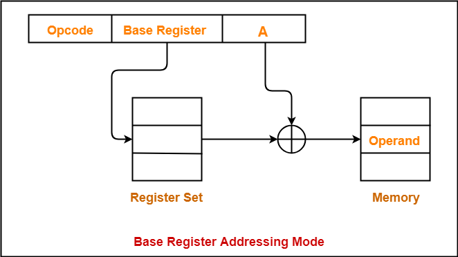
10. Base Register Addressing Mode-


In this addressing mode,

  • Effective address of the operand is obtained by adding the content of base register with the address part of the instruction.


Effective Address

= Content of Base Register + Address part of the instruction


11. Auto-Increment Addressing Mode-


  • This addressing mode is a special case of Register Indirect Addressing Mode where-


Effective Address of the Operand

= Content of Register


In this addressing mode,

  • After accessing the operand, the content of the register is automatically incremented by step size ‘d’.
  • Step size ‘d’ depends on the size of operand accessed.
  • Only one reference to memory is required to fetch the operand.


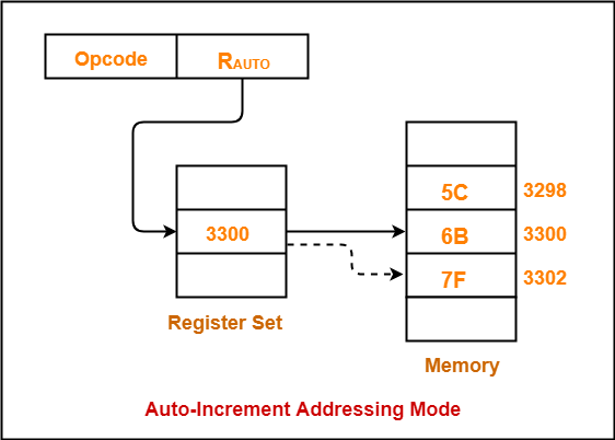
Example-


Assume operand size = 2 bytes.

Here,

  • After fetching the operand 6B, the instruction register RAUTO will be automatically incremented by 2.
  • Then, updated value of RAUTO will be 3300 + 2 = 3302.
  • At memory address 3302, the next operand will be found.


NOTE-


In auto-increment addressing mode,

  • First, the operand value is fetched.
  • Then, the instruction register RAUTO value is incremented by step size ‘d’.


12. Auto-Decrement Addressing Mode-


  • This addressing mode is again a special case of Register Indirect Addressing Mode where-


Effective Address of the Operand

Content of Register – Step Size


In this addressing mode,

  • First, the content of the register is decremented by step size ‘d’.
  • Step size ‘d’ depends on the size of operand accessed.
  • After decrementing, the operand is read.
  • Only one reference to memory is required to fetch the operand.


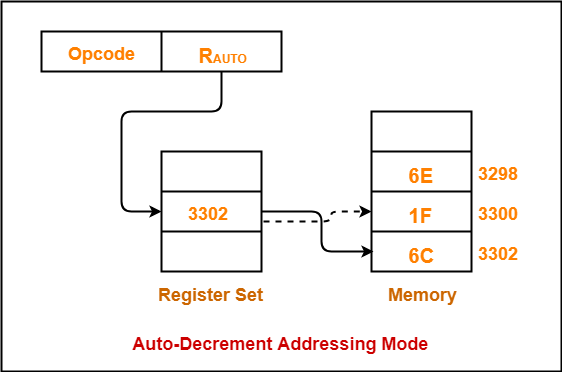
Example-


Assume operand size = 2 bytes.

Here,

  • First, the instruction register RAUTO will be decremented by 2.
  • Then, updated value of RAUTO will be 3302 – 2 = 3300.
  • At memory address 3300, the operand will be found.


NOTE-


In auto-decrement addressing mode,

  • First, the instruction register RAUTO value is decremented by step size ‘d’.
  • Then, the operand value is fetched.


Also Read- Practice Problems On Addressing Modes


Applications of Addressing Modes-


Addressing Modes Applications
Immediate Addressing Mode
  • To initialize registers to a constant value
Direct Addressing Mode

and

Register Direct Addressing Mode

  • To access static data
  • To implement variables
Indirect Addressing Mode

and

Register Indirect Addressing Mode

  • To implement pointers because pointers are memory locations that store the address of another variable
  • To pass array as a parameter because array name is the base address and pointer is needed to point the address
Relative Addressing Mode
  • For program relocation at run time i.e. for position independent code
  • To change the normal sequence of execution of instructions
  • For branch type instructions since it directly updates the program counter
Index Addressing Mode
  • For array implementation or array addressing
  • For records implementation
Base Register Addressing Mode
  • For writing relocatable code i.e. for relocation of program in memory even at run time
  • For handling recursive procedures
Auto-increment Addressing Mode

and

Auto-decrement Addressing Mode

  • For implementing loops
  • For stepping through arrays in a loop
  • For implementing a stack as push and pop


To gain better understanding about Addressing Modes,

Watch this Video Lecture


Next Article- Syntax Of Addressing Modes


Get more notes and other study material of Computer Organization and Architecture.

Watch video lectures by visiting our YouTube channel LearnVidFun.
Cache Memory in Computer Architecture

Cache Memory-


  • Cache memory is a Random Access Memory.
  • The main advantage of cache memory is its very fast speed.
  • It can be accessed by the CPU at much faster speed than main memory.


Location-


  • Cache memory lies on the path between the CPU and the main memory.
  • It facilitates the transfer of data between the processor and the main memory at the speed which matches to the speed of the processor.


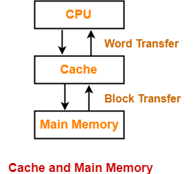
  • Data is transferred in the form of words between the cache memory and the CPU.
  • Data is transferred in the form of blocks or pages between the cache memory and the main memory.


Purpose-


  • The fast speed of the cache memory makes it extremely useful.
  • It is used for bridging the speed mismatch between the fastest CPU and the main memory.
  • It does not let the CPU performance suffer due to the slower speed of the main memory.


Execution Of Program-


  • Whenever any program has to be executed, it is first loaded in the main memory.
  • The portion of the program that is mostly probably going to be executed in the near future is kept in the cache memory.
  • This allows CPU to access the most probable portion at a faster speed.


Step-01:


Whenever CPU requires any word of memory, it is first searched in the CPU registers.

Now, there are two cases possible-


Case-01:


  • If the required word is found in the CPU registers, it is read from there.


Case-02:


  • If the required word is not found in the CPU registers, Step-02 is followed.


Step-02:


  • When the required word is not found in the CPU registers, it is searched in the cache memory.
  • Tag directory of the cache memory is used to search whether the required word is present in the cache memory or not.


Now, there are two cases possible-


Case-01:


  • If the required word is found in the cache memory, the word is delivered to the CPU.
  • This is known as Cache hit.


Case-02:


  • If the required word is not found in the cache memory, Step-03 is followed.
  • This is known as Cache miss.


Step-03:


  • When the required word is not found in the cache memory, it is searched in the main memory.
  • Page Table is used to determine whether the required page is present in the main memory or not.


Now, there are two cases possible-


Case-01:


If the page containing the required word is found in the main memory,

  • The page is mapped from the main memory to the cache memory.
  • This mapping is performed using cache mapping techniques.
  • Then, the required word is delivered to the CPU.


Case-02:


If the page containing the required word is not found in the main memory,

  • A page fault occurs.
  • The page containing the required word is mapped from the secondary memory to the main memory.
  • Then, the page is mapped from the main memory to the cache memory.
  • Then, the required word is delivered to the CPU.


Multilevel Cache Organization-


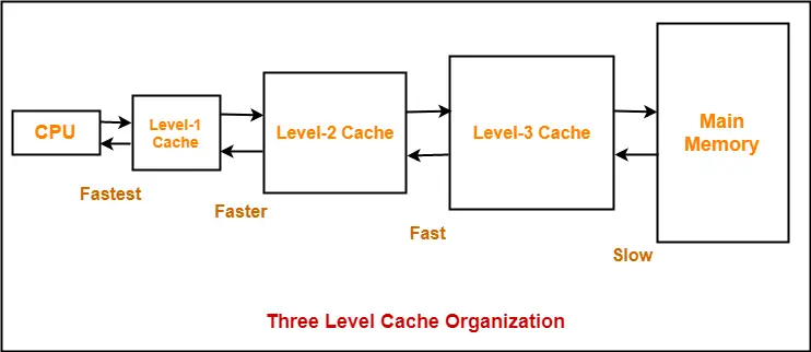
  • A multilevel cache organization is an organization where cache memories of different sizes are organized at multiple levels to increase the processing speed to a greater extent.
  • The smaller the size of cache, the faster its speed.
  • The smallest size cache memory is placed closest to the CPU.
  • This helps to achieve better performance in terms of speed.


Example-


Three level cache organization consists of three cache memories of different size organized at three different levels as shown below-


Size (L1 Cache) < Size (L2 Cache) < Size (L3 Cache) < Size (Main Memory)


To gain better understanding about Cache Memory,

Watch this Video Lecture


Next Article- Cache Mapping Techniques


Get more notes and other study material of Computer Organization and Architecture.

Watch video lectures by visiting our YouTube channel LearnVidFun.