Category: Computer Organization and Architecture

System Bus in Computer Architecture

System Bus in Computer Architecture-


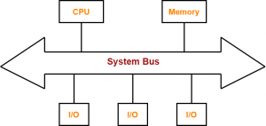
What Is A System Bus?


  • A bus is a set of electrical wires (lines) that connects the various hardware components of a computer system.
  • It works as a communication pathway through which information flows from one hardware component to the other hardware component.


A bus that connects major components (CPU, memory and I/O devices) of a computer system is called as a System Bus.


Why Do We Need Bus?


  • A computer system is made of different components such as memory, ALU, registers etc.
  • Each component should be able to communicate with other for proper execution of instructions and information flow.
  • If we try to implement a mesh topology among different components, it would be really expensive.
  • So, we use a common component to connect each necessary component i.e. BUS.


Components Of A System Bus-


The system bus consists of three major components-


  1. Data Bus
  2. Address Bus
  3. Control Bus


Let us learn about each component one by one.


1) Data Bus-


  • As the name suggests, data bus is used for transmitting the data / instruction from CPU to memory/IO and vice-versa.
  • It is bi-directional.


Data Bus Width


  • The width of a data bus refers to the number of bits (electrical wires) that the bus can carry at a time.
  • Each line carries 1 bit at a time. So, the number of lines in data bus determine how many bits can be transferred parallely.
  • The width of data bus is an important parameter because it determines how much data can be transmitted at one time.
  • The wider the bus width, faster would be the data flow on the data bus and thus better would be the system performance.


Examples-

  • A 32-bit bus has thirty two (32) wires and thus can transmit 32 bits of data at a time.
  • A 64-bit bus has sixty four (64) wires and thus can transmit 64 bits of data at a time.


2) Control Bus-


  • As the name suggests, control bus is used to transfer the control and timing signals from one component to the other component.
  • The CPU uses control bus to communicate with the devices that are connected to the computer system.
  • The CPU transmits different types of control signals to the system components.
  • It is bi-directional.


What Are Control & Timing Signals?


Control signals are generated in the control unit of CPU.

Timing signals are used to synchronize the memory and I/O operations with a CPU clock.


Typical control signals hold by control bus-

  • Memory read – Data from memory address location to be placed on data bus.
  • Memory write – Data from data bus to be placed on memory address location.
  • I/O Read – Data from I/O address location to be placed on data bus.
  • I/O Write – Data from data bus to be placed on I/O address location.


Other control signals hold by control bus are interrupt, interrupt acknowledge, bus request, bus grant and several others.

The type of action taking place on the system bus is indicated by these control signals.


Example-


When CPU wants to read or write data, it sends the memory read or memory write control signal on the control bus to perform the memory read or write operation from the main memory. Similarly, when the processor wants to read from an I/O device, it generates the I/O read signal.


3) Address Bus-


  • As the name suggests, address bus is used to carry address from CPU to memory/IO devices.
  • It is used to identify the particular location in memory.
  • It carries the source or destination address of data i.e. where to store or from where to retrieve the data.
  • It is uni-directional.


Example-


When CPU wants to read or write data, it sends the memory read or memory write control signal on the control bus to perform the memory read or write operation from the main memory and the address of the memory location is sent on the address bus.

If CPU wants to read data stored at the memory location (address) 4, the CPU send the value 4 in binary on the address bus.


Address Bus Width


  • The width of address bus determines the amount of physical memory addressable by the processor.
  • In other words, it determines the size of the memory that the computer can use.
  • The wider is the address bus, the more memory a computer will be able to use.
  •  The addressing capacity of the system can be increased by adding more address lines.


Examples-

  • An address bus that consists of 16 wires can convey 216 (= 64K) different addresses.
  • An address bus that consists of 32 wires can convey 232 (= 4G) different addresses.


PRACTICE PROBLEMS BASED ON SYSTEM BUS-


Problem-01:


Which of the following system bus is used to designate the source or destination of the data on the bus itself?

  1. Control bus
  2. Data bus
  3. Address bus
  4. System bus


Solution-


The correct option is (C) Address bus.

Address bus carries the source or destination address of data i.e. where to store or from where to retrieve the data.


Problem-02:


The bus which is used to transfer data from main memory to peripheral device is-

  1. Data bus
  2. Input bus
  3. DMA bus
  4. Output bus


Solution-


The correct option is (A) Data bus.

Data bus carries data / instruction from CPU to memory/IO and vice-versa.


Problem-03:


How many memory locations a system with a 32-bit address bus can address?

  1. 28
  2. 216
  3. 232
  4. 264


Solution-


The correct option is (C) 232.

232 memory locations can be addressed by a 32-bit address bus.


Problem-04:


How many bits can be transmitted at a time using a bus with 32 data lines?

  1. 8 bits
  2. 16 bits
  3. 32 bits
  4. 1024 bits


Solution-


Each line carries one bit. So, a bus with 32 data lines can transmit 32 bits at a time.


Problem-05:


A microprocessor has a data bus with 64 lines and an address bus with 32 lines. The maximum number of bits that can be stored in memory is-

  1. 32 x 212
  2. 32 x 264
  3. 64 x 232
  4. 64 x 264


Solution-


The correct option is (C) 64 x 232.

The amount of blocks that could be located is 232. Now, since data bus has 64 lines, so each block is 64 bits. Thus, maximum number of bits stored in memory is 232 x 64 bits.


Problem-06:


The address bus with a ROM of size 1024 x 8 bits is-

  1. 8 bits
  2. 10 bits
  3. 12 bits
  4. 16 bits


Solution-


The correct option is (B) 10 bits.

The size of the ROM is 1024 x 8 = 210 x 8. Here, 10 indicates the address bus and 8 indicates the data bus width.


Problem-07:


The data bus width of a ROM of size 2048 x 8 bits is-

  1. 8
  2. 10
  3. 12
  4. 16


Solution-


The correct option is (A) 8.

The size of the ROM is 2048 x 8 = 211 x 8. Here, 11 indicates the address bus and 8 indicates the data bus width.


To gain better understanding about System Bus in Computer Architecture,

Watch this Video Lecture


Next Article- Pipelining in Computer Architecture


Get more notes and other study material of Computer Organization and Architecture.

Watch video lectures by visiting our YouTube channel LearnVidFun.

Memory Organization in Computer Architecture

Memory Organization in Computer Architecture-


Before you go through this article, make sure that you have gone through the previous article on Memory Hierarchy.


In a computer,

  • Memory is organized at different levels.
  • CPU may try to access different levels of memory in different ways.
  • On this basis, the memory organization is broadly divided into two types-


  1. Simultaneous Access Memory Organization
  2. Hierarchical Access Memory Organization


1. Simultaneous Access Memory Organization-


In this memory organization,

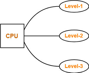
  • All the levels of memory are directly connected to the CPU.
  • Whenever CPU requires any word, it starts searching for it in all the levels simultaneously.


Example-01:


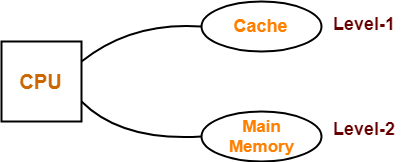
Consider the following simultaneous access memory organization-


Here, two levels of memory are directly connected to the CPU.


Let-

  • T1 = Access time of level L1
  • S1 = Size of level L1
  • C1 = Cost per byte of level L1
  • H1 = Hit rate of level L1

Similar are the notations for level L2.


Average Memory Access Time-


Average time required to access memory per operation

= H1 x T1 + (1 – H1) x H2 x T2

= H1 x T1 + (1 – H1) x 1 x T2

= H1 x T1 + (1 – H1) x T2


Important Note

In any memory organization,

  • The data item being searched will definitely be present in the last level.
  • Thus, hit rate for the last level is always 1.


Average Cost Per Byte-


Average cost per byte of the memory

= { C1 x S1 + C2 x S2 } / { S1 + S2 }


Example-02:


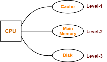
Consider the following simultaneous access memory organization-


Here, three levels of memory are directly connected to the CPU.


Let-

  • T1 = Access time of level L1
  • S1 = Size of level L1
  • C1 = Cost per byte of level L1
  • H1 = Hit rate of level L1

Similar are the notations for other two levels.


Average Memory Access Time-


Average time required to access memory per operation

= H1 x T1 + (1 – H1) x H2 x T2 + (1 – H1) x (1 – H2) x H3 x T3

= H1 x T1 + (1 – H1) x H2 x T2 + (1 – H1) x (1 – H2) x 1 x T3

= H1 x T1 + (1 – H1) x H2 x T2 + (1 – H1) x (1 – H2) x T3


Average Cost Per Byte-


Average cost per byte of the memory

= { C1 x S1 + C2 x S2 + C3 x S3 } / { S1 + S2 + S3 }


2. Hierarchical Access Memory Organization-


In this memory organization, memory levels are organized as-

  • Level-1 is directly connected to the CPU.
  • Level-2 is directly connected to level-1.
  • Level-3 is directly connected to level-2 and so on.


Whenever CPU requires any word,

  • It first searches for the word in level-1.
  • If the required word is not found in level-1, it searches for the word in level-2.
  • If the required word is not found in level-2, it searches for the word in level-3 and so on.


Example-01:


Consider the following hierarchical access memory organization-


Here, two levels of memory are connected to the CPU in a hierarchical fashion.


Let-

  • T1 = Access time of level L1
  • S1 = Size of level L1
  • C1 = Cost per byte of level L1
  • H1 = Hit rate of level L1

Similar are the notations for level L2.


Average Memory Access Time-


Average time required to access memory per operation

= H1 x T1 + (1 – H1) x H2 x (T1 + T2)

= H1 x T1 + (1 – H1) x 1 x (T1 + T2)

= H1 x T1 + (1 – H1) x (T1 + T2)


Average Cost Per Byte-


Average cost per byte of the memory

= { C1 x S1 + C2 x S2 } / { S1 + S2 }


Example-02:


Consider the following hierarchical access memory organization-


Here, three levels of memory are connected to the CPU in a hierarchical fashion.


Let-

  • T1 = Access time of level L1
  • S1 = Size of level L1
  • C1 = Cost per byte of level L1
  • H1 = Hit rate of level L1

Similar are the notations for other two levels.


Average Memory Access Time-


Average time required to access memory per operation

= H1 x T1 + (1 – H1) x H2 x (T1 + T2) + (1 – H1) x (1 – H2) x H3 x (T1 + T2 + T3)

= H1 x T1 + (1 – H1) x H2 x (T1 + T2) + (1 – H1) x (1 – H2) x 1 x (T1 + T2 + T3)

= H1 x T1 + (1 – H1) x H2 x (T1 + T2) + (1 – H1) x (1 – H2) x (T1 + T2 + T3)


Average Cost Per Byte-


Average cost per byte of the memory

= { C1 x S1 + C2 x S2 + C3 x S3 } / { S1 + S2 + S3 }


PRACTICE PROBLEMS BASED ON MEMORY ORGANIZATION-


Problem-01:


What is the average memory access time for a machine with a cache hit rate of 80% and cache access time of 5 ns and main memory access time of 100 ns when-

  1. Simultaneous access memory organization is used.
  2. Hierarchical access memory organization is used.


Solution-


Part-01: Simultaneous Access Memory Organization-


The memory organization will be as shown-


Average memory access time

= H1 x T1 + (1 – H1) x H2 x T2

= 0.8 x 5 ns + (1 – 0.8) x 1 x 100 ns

= 4 ns + 0.2 x 100 ns

= 4 ns + 20 ns

= 24 ns


Part-02: Hierarchical Access Memory Organization-


The memory organization will be as shown-


Average memory access time

= H1 x T1 + (1 – H1) x H2 x (T1 + T2)

= 0.8 x 5 ns + (1 – 0.8) x 1 x (5 ns + 100 ns)

= 4 ns + 0.2 x 10⁵ ns

= 4 ns + 21 ns

= 25 ns


Problem-02:


A computer has a cache, main memory and a disk used for virtual memory. An access to the cache takes 10 ns. An access to main memory takes 100 ns. An access to the disk takes 10,000 ns. Suppose the cache hit ratio is 0.9 and the main memory hit ratio is 0.8. The effective access time required to access a referenced word on the system is _______ when-

  1. Simultaneous access memory organization is used.
  2. Hierarchical access memory organization is used.


Solution-


Part-01:Simultaneous Access Memory Organization-


The memory organization will be as shown-


Effective memory access time

= H1 x T1 + (1 – H1) x H2 x T2 + (1 – H1) x (1 – H2) x H3 x T3

= 0.9 x 10 ns + (1 – 0.9) x 0.8 x 100 ns + (1 – 0.9) x (1 – 0.8) x 1 x 10000 ns

= 9 ns + 8 ns + 200 ns

= 217 ns


Part-02: Hierarchical Access Memory Organization-


The memory organization will be as shown-


Effective memory access time

= H1 x T1 + (1 – H1) x H2 x (T1 + T2) + (1 – H1) x (1 – H2) x H3 x (T1 + T2 + T3)

= 0.9 x 10 ns + (1 – 0.9) x 0.8 x (10 ns + 100 ns) + (1 – 0.9) x (1 – 0.8) x 1 x (10 ns + 100 ns + 10000 ns)

= 9 ns + 8.8 ns + 202.2 ns

= 220 ns


Important Note

While solving numerical problems

If the kind of memory organization used is not mentioned, assume hierarchical access memory organization.


To gain better understanding about Memory Organization,

Watch this Video Lecture


Next Article- Cache Memory


Get more notes and other study material of Computer Organization and Architecture.

Watch video lectures by visiting our YouTube channel LearnVidFun.

Pipelining | Practice Problems

Pipelining in Computer Architecture-


Before you go through this article, make sure that you have gone through the previous article on Instruction Pipelining.


In instruction pipelining,

  • A form of parallelism called as instruction level parallelism is implemented.
  • Multiple instructions execute simultaneously.
  • Speed up, Efficiency and Throughput serve as performance measures of pipelined execution.


Also Read- Performance Criteria Of Pipelining


In this article, we will discuss practice problems based on pipelining.


PRACTICE PROBLEMS BASED ON PIPELINING IN COMPUTER ARCHITECTURE-


Problem-01:


Consider a pipeline having 4 phases with duration 60, 50, 90 and 80 ns. Given latch delay is 10 ns. Calculate-

  1. Pipeline cycle time
  2. Non-pipeline execution time
  3. Speed up ratio
  4. Pipeline time for 1000 tasks
  5. Sequential time for 1000 tasks
  6. Throughput


Solution-


Given-

  • Four stage pipeline is used
  • Delay of stages = 60, 50, 90 and 80 ns
  • Latch delay or delay due to each register = 10 ns


Part-01: Pipeline Cycle Time-


Cycle time

= Maximum delay due to any stage + Delay due to its register

= Max { 60, 50, 90, 80 } + 10 ns

= 90 ns + 10 ns

= 100 ns


Part-02: Non-Pipeline Execution Time-


Non-pipeline execution time for one instruction

= 60 ns + 50 ns + 90 ns + 80 ns

= 280 ns


Part-03: Speed Up Ratio-


Speed up

= Non-pipeline execution time / Pipeline execution time

= 280 ns / Cycle time

= 280 ns / 100 ns

= 2.8


Part-04: Pipeline Time For 1000 Tasks-


Pipeline time for 1000 tasks

= Time taken for 1st task + Time taken for remaining 999 tasks

= 1 x 4 clock cycles + 999 x 1 clock cycle

= 4 x cycle time + 999 x cycle time

= 4 x 100 ns + 999 x 100 ns

= 400 ns + 99900 ns

= 100300 ns


Part-05: Sequential Time For 1000 Tasks-


Non-pipeline time for 1000 tasks

= 1000 x Time taken for one task

= 1000 x 280 ns

= 280000 ns


Part-06: Throughput-


Throughput for pipelined execution

= Number of instructions executed per unit time

= 1000 tasks / 100300 ns


Problem-02:


A four stage pipeline has the stage delays as 150, 120, 160 and 140 ns respectively. Registers are used between the stages and have a delay of 5 ns each. Assuming constant clocking rate, the total time taken to process 1000 data items on the pipeline will be-

  1. 120.4 microseconds
  2. 160.5 microseconds
  3. 165.5 microseconds
  4. 590.0 microseconds


Solution-


Given-

  • Four stage pipeline is used
  • Delay of stages = 150, 120, 160 and 140 ns
  • Delay due to each register = 5 ns
  • 1000 data items or instructions are processed


Cycle Time-


Cycle time

= Maximum delay due to any stage + Delay due to its register

= Max { 150, 120, 160, 140 } + 5 ns

= 160 ns + 5 ns

= 165 ns


Pipeline Time To Process 1000 Data Items-


Pipeline time to process 1000 data items

= Time taken for 1st data item + Time taken for remaining 999 data items

= 1 x 4 clock cycles + 999 x 1 clock cycle

= 4 x cycle time + 999 x cycle time

= 4 x 165 ns + 999 x 165 ns

= 660 ns + 164835 ns

= 165495 ns

= 165.5 μs

Thus, Option (C) is correct.


Problem-03:


Consider a non-pipelined processor with a clock rate of 2.5 gigahertz and average cycles per instruction of 4. The same processor is upgraded to a pipelined processor with five stages but due to the internal pipeline delay, the clock speed is reduced to 2 gigahertz. Assume there are no stalls in the pipeline. The speed up achieved in this pipelined processor is-

  1. 3.2
  2. 3.0
  3. 2.2
  4. 2.0


Solution-


Cycle Time in Non-Pipelined Processor-


Frequency of the clock = 2.5 gigahertz

Cycle time

= 1 / frequency

= 1 / (2.5 gigahertz)

= 1 / (2.5 x 10⁹ hertz)

= 0.4 ns


Non-Pipeline Execution Time-


Non-pipeline execution time to process 1 instruction

= Number of clock cycles taken to execute one instruction

= 4 clock cycles

= 4 x 0.4 ns

= 1.6 ns


Cycle Time in Pipelined Processor-


Frequency of the clock = 2 gigahertz

Cycle time

= 1 / frequency

= 1 / (2 gigahertz)

= 1 / (2 x 10⁹ hertz)

= 0.5 ns


Pipeline Execution Time-


Since there are no stalls in the pipeline, so ideally one instruction is executed per clock cycle. So,

Pipeline execution time

= 1 clock cycle

= 0.5 ns


Speed Up-


Speed up

= Non-pipeline execution time / Pipeline execution time

= 1.6 ns / 0.5 ns

= 3.2

Thus, Option (A) is correct.


Problem-04:


The stage delays in a 4 stage pipeline are 800, 500, 400 and 300 picoseconds. The first stage is replaced with a functionally equivalent design involving two stages with respective delays 600 and 350 picoseconds.

The throughput increase of the pipeline is _____%.


Solution-


Execution Time in 4 Stage Pipeline-


Cycle time

= Maximum delay due to any stage + Delay due to its register

= Max { 800, 500, 400, 300 } + 0

= 800 picoseconds

Thus, Execution time in 4 stage pipeline = 1 clock cycle = 800 picoseconds.


Throughput in 4 Stage Pipeline-


Throughput

= Number of instructions executed per unit time

= 1 instruction / 800 picoseconds


Execution Time in 2 Stage Pipeline-


Cycle time

= Maximum delay due to any stage + Delay due to its register

= Max { 600, 350 } + 0

= 600 picoseconds

Thus, Execution time in 2 stage pipeline = 1 clock cycle = 600 picoseconds.


Throughput in 2 Stage Pipeline-


Throughput

= Number of instructions executed per unit time

= 1 instruction / 600 picoseconds


Throughput Increase-


Throughput increase

= { (Final throughput – Initial throughput) / Initial throughput } x 100

= { (1 / 600 – 1 / 800) / (1 / 800) } x 100

= { (800 / 600) – 1 } x 100

= (1.33 – 1) x 100

= 0.3333 x 100

= 33.33 %


Problem-05:


A non-pipelined single cycle processor operating at 100 MHz is converted into a synchronous pipelined processor with five stages requiring 2.5 ns, 1.5 ns, 2 ns, 1.5 ns and 2.5 ns respectively. The delay of the latches is 0.5 sec.

The speed up of the pipeline processor for a large number of instructions is-

  1. 4.5
  2. 4.0
  3. 3.33
  4. 3.0


Solution-


Cycle Time in Non-Pipelined Processor-


Frequency of the clock = 100 MHz

Cycle time

= 1 / frequency

= 1 / (100 MHz)

= 1 / (100 x 106 hertz)

= 0.01 μs


Non-Pipeline Execution Time-


Non-pipeline execution time to process 1 instruction

= Number of clock cycles taken to execute one instruction

= 1 clock cycle

= 0.01 μs

= 10 ns


Cycle Time in Pipelined Processor-


Cycle time

= Maximum delay due to any stage + Delay due to its register

= Max { 2.5, 1.5, 2, 1.5, 2.5 } + 0.5 ns

= 2.5 ns + 0.5 ns

= 3 ns


Pipeline Execution Time-


Pipeline execution time

= 1 clock cycle

= 3 ns


Speed Up-


Speed up

= Non-pipeline execution time / Pipeline execution time

= 10 ns / 3 ns

= 3.33

Thus, Option (C) is correct.


Problem-06:


We have 2 designs D1 and D2 for a synchronous pipeline processor. D1 has 5 stage pipeline with execution time of 3 ns, 2 ns, 4 ns, 2 ns and 3 ns. While the design D2 has 8 pipeline stages each with 2 ns execution time. How much time can be saved using design D2 over design D1 for executing 100 instructions?

  1. 214 ns
  2. 202 ns
  3. 86 ns
  4. 200 ns


Solution-


Cycle Time in Design D1-


Cycle time

= Maximum delay due to any stage + Delay due to its register

= Max { 3, 2, 4, 2, 3 } + 0

= 4 ns


Execution Time For 100 Instructions in Design D1-


Execution time for 100 instructions

= Time taken for 1st instruction + Time taken for remaining 99 instructions

= 1 x 5 clock cycles + 99 x 1 clock cycle

= 5 x cycle time + 99 x cycle time

= 5 x 4 ns + 99 x 4 ns

= 20 ns + 396 ns

= 416 ns


Cycle Time in Design D2-


Cycle time

= Delay due to a stage + Delay due to its register

= 2 ns + 0

= 2 ns


Execution Time For 100 Instructions in Design D2-


Execution time for 100 instructions

= Time taken for 1st instruction + Time taken for remaining 99 instructions

= 1 x 8 clock cycles + 99 x 1 clock cycle

= 8 x cycle time + 99 x cycle time

= 8 x 2 ns + 99 x 2 ns

= 16 ns + 198 ns

= 214 ns


Time Saved-


Time saved

= Execution time in design D1 – Execution time in design D2

= 416 ns – 214 ns

= 202 ns

Thus, Option (B) is correct.


Problem-07:


Consider an instruction pipeline with four stages (S1, S2, S3 and S4) each with combinational circuit only. The pipeline registers are required between each stage and at the end of the last stage. Delays for the stages and for the pipeline registers are as given in the figure-
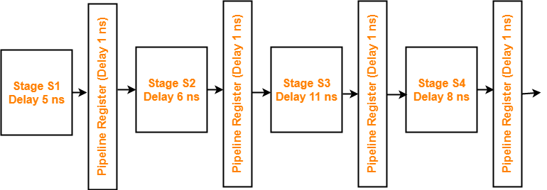


What is the approximate speed up of the pipeline in steady state under ideal conditions when compared to the corresponding non-pipeline implementation?

  1. 4.0
  2. 2.5
  3. 1.1
  4. 3.0


Solution-


Non-Pipeline Execution Time-


Non-pipeline execution time for 1 instruction

= 5 ns + 6 ns + 11 ns + 8 ns

= 30 ns


Cycle Time in Pipelined Processor-


Cycle time

= Maximum delay due to any stage + Delay due to its register

= Max { 5, 6, 11, 8 } + 1 ns

= 11 ns + 1 ns

= 12 ns


Pipeline Execution Time-


Pipeline execution time

= 1 clock cycle

= 12 ns


Speed Up-


Speed up

= Non-pipeline execution time / Pipeline execution time

= 30 ns / 12 ns

= 2.5

Thus, Option (B) is correct.


Problem-08:


Consider a 4 stage pipeline processor. The number of cycles needed by the four instructions I1, I2, I3 and I4 in stages S1, S2, S3 and S4 is shown below-


S1 S2 S3 S4
I1 2 1 1 1
I2 1 3 2 2
I3 2 1 1 3
I4 1 2 2 2


What is the number of cycles needed to execute the following loop?

for(i=1 to 2) { I1; I2; I3; I4; }

  1. 16
  2. 23
  3. 28
  4. 30


Solution-


The phase-time diagram is-


From here, number of clock cycles required to execute the loop = 23 clock cycles.

Thus, Option (B) is correct.


Problem-09:


Consider a pipelined processor with the following four stages-

IF : Instruction Fetch

ID : Instruction Decode and Operand Fetch

EX : Execute

WB : Write Back


The IF, ID and WB stages take one clock cycle each to complete the operation. The number of clock cycles for the EX stage depends on the instruction. The ADD and SUB instructions need 1 clock cycle and the MUL instruction need 3 clock cycles in the EX stage. Operand forwarding is used in the pipelined processor. What is the number of clock cycles taken to complete the following sequence of instructions?


ADD R2, R1, R0      R2 ← R0 + R1

MUL R4, R3, R2      R4 ← R3 + R2

SUB R6, R5, R4      R6 ← R5 + R4


  1. 7
  2. 8
  3. 10
  4. 14


Solution-


The phase-time diagram is-
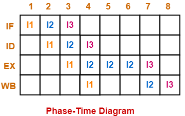


From here, number of clock cycles required to execute the instructions = 8 clock cycles.

Thus, Option (B) is correct.


Problem-10:


Consider the following procedures. Assume that the pipeline registers have zero latency.

P1 : 4 stage pipeline with stage latencies 1 ns, 2 ns, 2 ns, 1 ns

P2 : 4 stage pipeline with stage latencies 1 ns, 1.5 ns, 1.5 ns, 1.5 ns

P3 : 5 stage pipeline with stage latencies 0.5 ns, 1 ns, 1 ns, 0.6 ns, 1 ns

P4 : 5 stage pipeline with stage latencies 0.5 ns, 0.5 ns, 1 ns, 1 ns, 1.1 ns


Which procedure has the highest peak clock frequency?

  1. P1
  2. P2
  3. P3
  4. P4


Solution-


It is given that pipeline registers have zero latency. Thus,

Cycle time

= Maximum delay due to any stage + Delay due to its register

= Maximum delay due to any stage


For Processor P1:


Cycle time

= Max { 1 ns, 2 ns, 2 ns, 1 ns }

= 2 ns


Clock frequency

= 1 / Cycle time

= 1 / 2 ns

= 0.5 gigahertz


For Processor P2:


Cycle time

= Max { 1 ns, 1.5 ns, 1.5 ns, 1.5 ns }

= 1.5 ns


Clock frequency

= 1 / Cycle time

= 1 / 1.5 ns

= 0.67 gigahertz


For Processor P3:


Cycle time

= Max { 0.5 ns, 1 ns, 1 ns, 0.6 ns, 1 ns }

= 1 ns


Clock frequency

= 1 / Cycle time

= 1 / 1 ns

= 1 gigahertz


For Processor P4:


Cycle time

= Max { 0.5 ns, 0.5 ns, 1 ns, 1 ns, 1.1 ns }

= 1.1 ns


Clock frequency

= 1 / Cycle time

= 1 / 1.1 ns

= 0.91 gigahertz


Clearly, Process P3 has the highest peak clock frequency.

Thus, Option (C) is correct.


Problem-11:


Consider a 3 GHz (gigahertz) processor with a three-stage pipeline and stage latencies T1, T2 and T3 such that T1 = 3T2/4 = 2T3. If the longest pipeline stage is split into two pipeline stages of equal latency, the new frequency is ____ GHz, ignoring delays in the pipeline registers.


Solution-


Let ‘t’ be the common multiple of each ratio, then-

  • T1 = t
  • T2 = 4t / 3
  • T3 = t / 2


Pipeline Cycle Time-


Pipeline cycle time

= Maximum delay due to any stage + Delay due to its register

= Max { t, 4t/3, t/2 } + 0

= 4t/3


Frequency Of Pipeline-


Frequency

= 1 / Pipeline cycle time

= 1 / (4t / 3)

= 3 / 4t


Given frequency = 3 GHz. So,

3 / 4t = 3 GHz

4t = 1 ns

t = 0.25 ns


Stage Latencies Of Pipeline-


Stage latency of different stages are-

  • Latency of stage-01 = 0.25 ns
  • Latency of stage-02 = 0.33 ns
  • Latency of stage-03 = 0.125 ns


Splitting The Pipeline-


The stage with longest latency i.e. stage-02 is split up into 4 stages.

After splitting, the latency of different stages are-

  • Latency of stage-01 = 0.25 ns
  • Latency of stage-02 = 0.165 ns
  • Latency of stage-03 = 0.165 ns
  • Latency of stage-04 = 0.125 ns


Splitted Pipeline Cycle Time-


Splitted pipeline cycle time

= Maximum delay due to any stage + Delay due to its register

= Max { 0.25, 0.165, 0.165, 0.125 } + 0

= 0.25 ns


Frequency Of Splitted Pipeline-


Frequency

= 1 / splitted pipeline cycle time

= 1 / 0.25 ns

= 4 GHz

Thus, new frequency = 4 GHz.


Get more notes and other study material of Computer Organization and Architecture.

Watch video lectures by visiting our YouTube channel LearnVidFun.
Instruction Pipelining | Performance

Instruction Pipelining-


Before you go through this article, make sure that you have gone through the previous article on Instruction Pipelining.


In instruction pipelining,

  • A form of parallelism called as instruction level parallelism is implemented.
  • Multiple instructions execute simultaneously.
  • The efficiency of pipelined execution is more than that of non-pipelined execution.


Performance of Pipelined Execution-


The following parameters serve as criterion to estimate the performance of pipelined execution-

  • Speed Up
  • Efficiency
  • Throughput


1. Speed Up-


It gives an idea of “how much faster” the pipelined execution is as compared to non-pipelined execution.

It is calculated as-


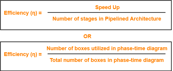
2. Efficiency-


The efficiency of pipelined execution is calculated as-


3. Throughput-


Throughput is defined as number of instructions executed per unit time.

It is calculated as-


Calculation of Important Parameters-


Let us learn how to calculate certain important parameters of pipelined architecture.

Consider-

  • A pipelined architecture consisting of k-stage pipeline
  • Total number of instructions to be executed = n


Point-01: Calculating Cycle Time-


In pipelined architecture,

  • There is a global clock that synchronizes the working of all the stages.
  • Frequency of the clock is set such that all the stages are synchronized.
  • At the beginning of each clock cycle, each stage reads the data from its register and process it.
  • Cycle time is the value of one clock cycle.


There are two cases possible-


Case-01: All the stages offer same delay-


If all the stages offer same delay, then-

Cycle time = Delay offered by one stage including the delay due to its register


Case-02: All the stages do not offer same delay-


If all the stages do not offer same delay, then-

Cycle time = Maximum delay offered by any stage including the delay due to its register


Point-02: Calculating Frequency Of Clock-


Frequency of the clock (f) = 1 / Cycle time


Point-03: Calculating Non-Pipelined Execution Time-


In non-pipelined architecture,

  • The instructions execute one after the other.
  • The execution of a new instruction begins only after the previous instruction has executed completely.
  • So, number of clock cycles taken by each instruction = k clock cycles


Thus,

Non-pipelined execution time

= Total number of instructions x Time taken to execute one instruction

= n x k clock cycles


Point-04: Calculating Pipelined Execution Time-


In pipelined architecture,

  • Multiple instructions execute parallely.
  • Number of clock cycles taken by the first instruction = k clock cycles
  • After first instruction has completely executed, one instruction comes out per clock cycle.
  • So, number of clock cycles taken by each remaining instruction = 1 clock cycle


Thus,

Pipelined execution time

= Time taken to execute first instruction + Time taken to execute remaining instructions

= 1 x k clock cycles + (n-1) x 1 clock cycle

= (k + n – 1) clock cycles


Point-04: Calculating Speed Up-


Speed up

= Non-pipelined execution time / Pipelined execution time

= n x k clock cycles / (k + n – 1) clock cycles

= n x k / (k + n – 1)

= n x k / n + (k – 1)

= k / { 1 + (k – 1)/n }


  • For very large number of instructions, n→∞. Thus, speed up = k.
  • Practically, total number of instructions never tend to infinity.
  • Therefore, speed up is always less than number of stages in pipeline.


Important Notes-


Note-01:


  • The aim of pipelined architecture is to execute one complete instruction in one clock cycle.
  • In other words, the aim of pipelining is to maintain CPI ≅ 1.
  • Practically, it is not possible to achieve CPI ≅ 1 due to delays that get introduced due to registers.
  • Ideally, a pipelined architecture executes one complete instruction per clock cycle (CPI=1).


Note-02:


  • The maximum speed up that can be achieved is always equal to the number of stages.
  • This is achieved when efficiency becomes 100%.
  • Practically, efficiency is always less than 100%.
  • Therefore speed up is always less than number of stages in pipelined architecture.


Note-03:


Under ideal conditions,

  • One complete instruction is executed per clock cycle i.e. CPI = 1.
  • Speed up = Number of stages in pipelined architecture


Note-04:


  • Experiments show that 5 stage pipelined processor gives the best performance.


Note-05:


In case only one instruction has to be executed, then-

  • Non-pipelined execution gives better performance than pipelined execution.
  • This is because delays are introduced due to registers in pipelined architecture.
  • Thus, time taken to execute one instruction in non-pipelined architecture is less.


Note-06:


High efficiency of pipelined processor is achieved when-

  • All the stages are of equal duration.
  • There are no conditional branch instructions.
  • There are no interrupts.
  • There are no register and memory conflicts.

Performance degrades in absence of these conditions.


To gain better understanding about Pipelining in Computer Architecture,

Watch this Video Lecture


Next Article- Practice Problems On Pipelining


Get more notes and other study material of Computer Organization and Architecture.

Watch video lectures by visiting our YouTube channel LearnVidFun.

Pipelining in Computer Architecture

Introduction-


  • A program consists of several number of instructions.
  • These instructions may be executed in the following two ways-


  1. Non-Pipelined Execution
  2. Pipelined Execution


1. Non-Pipelined Execution-


In non-pipelined architecture,

  • All the instructions of a program are executed sequentially one after the other.
  • A new instruction executes only after the previous instruction has executed completely.
  • This style of executing the instructions is highly inefficient.


Example-


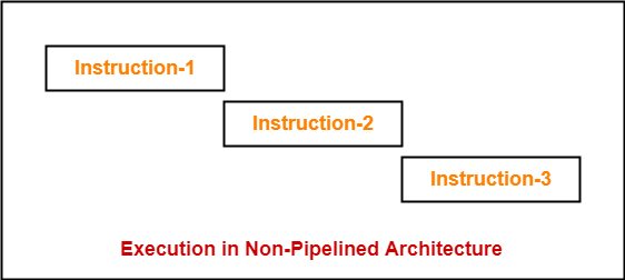
Consider a program consisting of three instructions.

In a non-pipelined architecture, these instructions execute one after the other as-


If time taken for executing one instruction = t, then-

Time taken for executing ‘n’ instructions = n x t


2. Pipelined Execution-


In pipelined architecture,

  • Multiple instructions are executed parallely.
  • This style of executing the instructions is highly efficient.


Now, let us discuss instruction pipelining in detail.


Instruction Pipelining-


Instruction pipelining is a technique that implements a form of parallelism called as instruction level parallelism within a single processor.


  • A pipelined processor does not wait until the previous instruction has executed completely.
  • Rather, it fetches the next instruction and begins its execution.


Pipelined Architecture-


In pipelined architecture,

  • The hardware of the CPU is split up into several functional units.
  • Each functional unit performs a dedicated task.
  • The number of functional units may vary from processor to processor.
  • These functional units are called as stages of the pipeline.
  • Control unit manages all the stages using control signals.
  • There is a register associated with each stage that holds the data.
  • There is a global clock that synchronizes the working of all the stages.
  • At the beginning of each clock cycle, each stage takes the input from its register.
  • Each stage then processes the data and feed its output to the register of the next stage.


Four-Stage Pipeline-


In four stage pipelined architecture, the execution of each instruction is completed in following 4 stages-

  1. Instruction fetch (IF)
  2. Instruction decode (ID)
  3. Instruction Execute (IE)
  4. Write back (WB)


To implement four stage pipeline,

  • The hardware of the CPU is divided into four functional units.
  • Each functional unit performs a dedicated task.


Stage-01:


At stage-01,

  • First functional unit performs instruction fetch.
  • It fetches the instruction to be executed.


Stage-02:


At stage-02,

  • Second functional unit performs instruction decode.
  • It decodes the instruction to be executed.


Stage-03:


At stage-03,

  • Third functional unit performs instruction execution.
  • It executes the instruction.


Stage-04:


At stage-04,

  • Fourth functional unit performs write back.
  • It writes back the result so obtained after executing the instruction.


Execution-


In pipelined architecture,

  • Instructions of the program execute parallely.
  • When one instruction goes from nth stage to (n+1)th stage, another instruction goes from (n-1)th stage to nth stage.


Phase-Time Diagram-


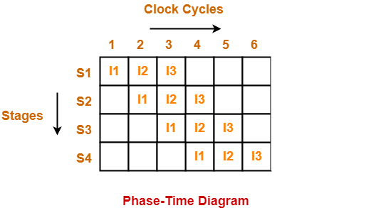
  • Phase-time diagram shows the execution of instructions in the pipelined architecture.
  • The following diagram shows the execution of three instructions in four stage pipeline architecture.


Time taken to execute three instructions in four stage pipelined architecture = 6 clock cycles.


NOTE-


In non-pipelined architecture,

Time taken to execute three instructions would be

= 3 x Time taken to execute one instruction

= 3 x 4 clock cycles

= 12 clock cycles

Clearly, pipelined execution of instructions is far more efficient than non-pipelined execution.


To gain better understanding about Pipelining in Computer Architecture,

Watch this Video Lecture


Next Article- Instruction Pipeline | Formulas


Get more notes and other study material of Computer Organization and Architecture.

Watch video lectures by visiting our YouTube channel LearnVidFun.